Skip to product information
Shop now


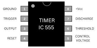
555 Timer IC – Pin Diagram & Pin Configuration Guide | radiomarket.in
Sale price
Rs. 10.00
Regular price
Rs. 15.00
Shipping calculated at checkout.
Pickup currently not available
The 555 Timer IC is one of the most popular integrated circuits used in electronics projects for timing, pulse generation, and oscillation applications. Understanding the pin diagram and configuration is essential for designing circuits like LED blinkers, timers, frequency generators, and delay circuits.
This guide from radiomarket.in provides clear details about all 8 pins of the 555 IC, their functions, and typical applications. Ideal for students, hobbyists, and electronics enthusiasts, it helps in accurate and efficient circuit design.
⚙️ Key Features:
-
Detailed pin diagram of 555 Timer IC
-
Explanation of all 8 pins: GND, VCC, Trigger, Output, Reset, Control Voltage, Threshold, Discharge
-
Examples for astable and monostable circuits
-
Ideal for learning, project building, and DIY electronics
-
Compact reference for students, engineers, and hobbyists
📊 Pin Configuration:
-
GND – Ground reference
-
VCC – Supply voltage (4.5V–15V)
-
Trigger – Activates output when voltage falls below 1/3 VCC
-
Output – Output of the timer
-
Control Voltage – Modifies threshold and trigger voltage
-
Threshold – Ends the timing interval in monostable mode
-
Discharge – Discharges the timing capacitor
-
Reset – Resets the timer when pulled low
Details
This product is crafted with quality materials to ensure durability and performance. Designed with your convenience in mind, it seamlessly fits into your everyday life.
Shipping & Returns
We strive to process and ship all orders in a timely manner, working diligently to ensure that your items are on their way to you as soon as possible.
We are committed to ensuring a positive shopping experience for all our customers. If for any reason you wish to return an item, we invite you to reach out to our team for assistance, and we will evaluate every return request with care and consideration.
Shop The Full Collection